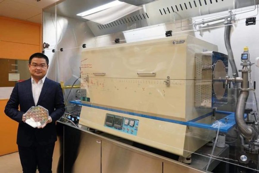
MIT Engineers Revolutionize Semiconductor Chip Technology With Atom-Thin Transistors
Researchers at MIT have developed a new low-temperature growth process that can integrate 2D materials onto silicon circuits, allowing for denser and more powerful semiconductors. Traditional semiconductor chips are made with bulk materials, which are difficult to stack to create denser integrations, but 2D materials could be stacked to create more powerful chips.

Researchers at MIT have developed a new low-temperature growth process that can integrate 2D materials onto silicon circuits, allowing for denser and more powerful semiconductors. Traditional semiconductor chips are made with bulk materials, which are difficult to stack to create denser integrations, but 2D materials could be stacked to create more powerful chips. However, growing 2D materials directly onto a silicon chip typically requires high temperatures that could damage the chip. The new technology bypasses this challenge by growing 2D transition metal dichalcogenide (TMD) materials directly on top of a fully fabricated silicon chip without damaging it. The new process allows for uniform layers across larger 8-inch wafers and significantly reduces growth time, making it better-suited for commercial applications. The integration of 2D materials onto a silicon chip could increase the density of an integrated circuit, leading to amazing new things. The research was published in the journal Nature Nanotechnology.
The interdisciplinary team of researchers developed a low-temperature growth process that grows a smooth and highly uniform layer of 2D materials across an entire 8-inch wafer in less than an hour, significantly reducing the time it takes to grow these materials. This method is a departure from previous approaches that required growing 2D materials elsewhere and then transferring them onto a chip or a wafer, which often resulted in imperfections that affected the performance of the final devices and circuits.
The new technique is expected to pave the way for the creation of more powerful chips that are vital for emerging AI applications, such as chatbots that generate natural human language. This breakthrough comes at a time when the semiconductor industry is experiencing a shortage of chips, and demand for more powerful and efficient semiconductors continues to grow.
The technology has been tested successfully, demonstrating the ability to grow 2D materials directly onto much larger surfaces than previously demonstrated, making it well-suited for commercial applications. The team is excited about the potential for their method to revolutionize the semiconductor industry and enable the creation of more powerful and energy-efficient chips that can meet the demands of modern applications.
Reference: https://scitechdaily.com/mit-engineers-revolutionize-semiconductor-chip-technology-with-atom-thin-transistors/
What's Your Reaction?


/https://tf-cmsv2-smithsonianmag-media.s3.amazonaws.com/filer_public/54/66/546650fa-26a4-40fd-8d6d-5a7a04540f81/rosetta2.png)
:max_bytes(150000):strip_icc():focal(999x0:1001x2)/robert-prevost-050825-1-39395418ab494da5a3a700c9478e66c8.jpg)


format(webp))
format(webp))


